Die Sorter
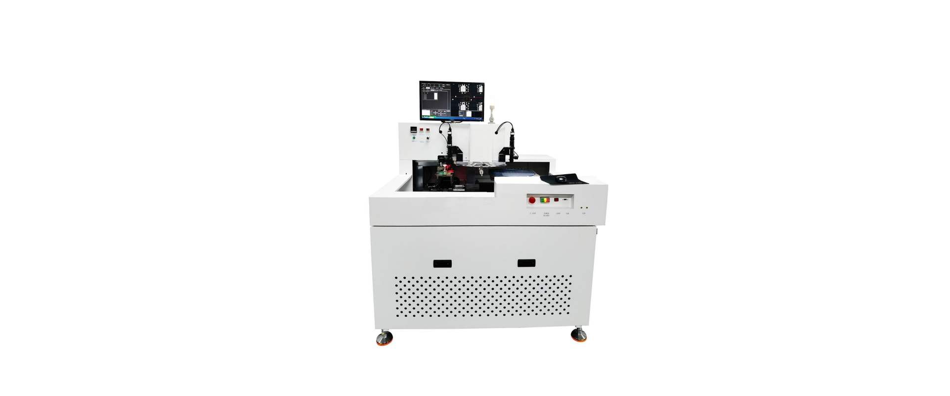
Wafer to Waffle Pack Die Sorter HJC-560T
Automatic wafer to waffle pack die sorting machine with mapping. Waffer automatic loading and unloading is optional. 2×2 or 4×4 waffle pak automatic loading/unloading with magazine is optional. Machine pick die from wafer and place to waffle pack, Gel-Pak, JEDEC tray or custom tray.
Machine Features:
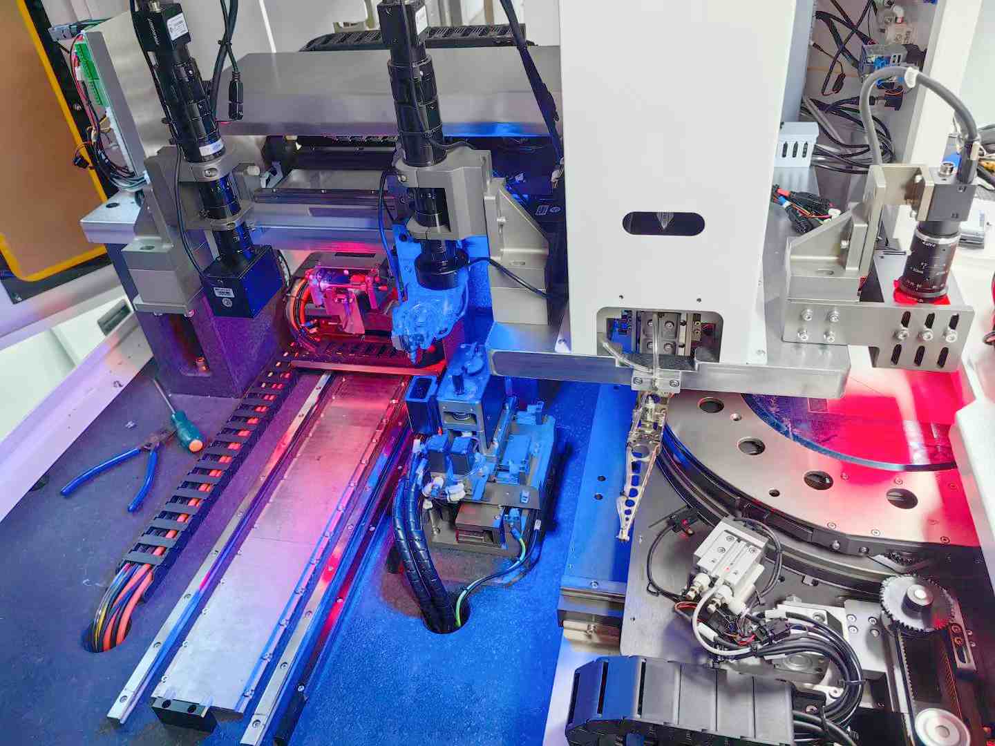
- The servo direct-connected 180-degree pick-and-place head can be customized freely for 6-inch, 8-inch and 12-inch wafers, as well as sub-rings and iron rings;
- According to the wafer size (L,W,H), customized multi-thimble or single thimble mechanism;
- The wafer workbench can be equipped with an ion fan;
- Automatic search mechanism of wafer table, which automatically forms search track;
- Automatically searches for die according to the Mapping file.
- Special vacuum suction nozzle with large suction;
- Multi-sucker vacuum fixture with large suction;
- Using vacuum leak detection;
- Waffle placing inspection function;
- Identify defective chips such as missing corners and ink spots;
- Simple visual operation interface simplifies the operation;

High-Precision Wafer to waffle machine
Solution can be customized
Waffle tray or JEDEC tray
Can be flip chip
Loading/unloading can be automatic
Can have mapping function
Re:Wafer to Waffle Pack Machine HJC-560T
| 1. System functions | 4. Die suction swing arm | ||
| Speed | UPH:10K+/H (related to wafer size and blue film viscosity, subject to actual test results). | Swing arm | 180 rotatable |
| XY position accuracy | ±25um | Suction pressure | Adjustable 30g—300g |
| Chip rotation | ±3° | 5. Wafer platform | |
| 2. Chip XY workbench | Range of travel stroke | Customized | |
| Chip size | 0.2mm×0.2mm-5mm×5mm (more size can be compatible by changing the lens barrel). | XY resolution | 0.02mil |
| Maximum chip ring size | 6 “(other sizes can be customized). | 6. Required facilities | |
| Maximum chip area size | 4″ | Voltage/frequency | 220V AC±5%/50HZ |
| Resolution ratio | 0.04mil | Compressed air | 0.5MPa(MIN) |
| Z height stroke of thimble | 4mm / Resolution: 0.04mil | Rated power | 800W |
| 3. Image recognition system | Gas consumption | 5L/min | |
| Gray scale | 256 gray scale | 7. Size and weight | |
| resolution ratio | 752×480 pixels (maximum 130W pixels) | Long x wide x high | 130×120×170cm |
| Accuracy of image recognition | ±0.025mil@50mil observation range | Weight | 630kg |
Wafer bonding | Chip handling equipment | Die attach process | Die bonder machine | Die sorting technology | Flip chip bonding | Chip handling equipment | die sorter | semiconductor die sorter | automated die sorter | wafer die sorter | die sorting equipment | die bonding and sorting | high speed die sorter | wafer mapping | die bonder | semiconductor die bonder | automated die bonder | die bonding equipment | die bonder machine | high precision die bonder | die attach | semiconductor die attach | automated die attach | die attach process | eutectic die bonder | epoxy die bonder | die sorting machine | automated die sorting machine | high speed die sorting machine | precision die sorting machine | flip chip die sorting | MEMS die bonding | sintering bonding | IGBT bonding equipment | EEL COB Epoxy bonding | Multi dies and different angle bonding | FMCW Mixed packaging | multi chip COC eutectic | Heating tip flip chip bonding | CoS/Bar eutectic | Single COS to Box Eutectic | PA device bonding | Multi channel Lens passive bonding | Bare die to tape and reel machine | wafer to tape and reel | wafer to waffle | wafer to tray | atomic force microscope
